A comprehensive Guide About PCB Prototyping.
Introduction
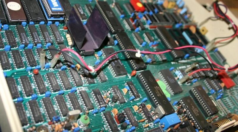
Printed Circuit Board (PCB) prototyping is the process of designing and creating a physical sample of a printed circuit board design. It is an essential step in the development of any electronic device and is used to test and verify the functionality of the design. PCB prototyping is a critical part of the product development cycle and can save time and money by allowing designers to identify and correct issues before mass production begins.
Design Process
The design process for a PCB prototype starts with the creation of a schematic, which is a visual representation of the electrical connections and components used in the design. The schematic is then converted into a PCB layout using computer-aided design (CAD) software, which allows the designer to place the components and route the connections on the board.
Once the design is complete, it is sent to a PCB manufacturer for production. The manufacturer uses a variety of methods to transfer the design onto the PCB material, including photo-lithography, etching, and drilling. After the design is transferred onto the board, the components are soldered into place and the board is tested to ensure that it functions as intended.
Materials and Methods
There are several materials and methods used in PCB prototyping, each with its own unique advantages and disadvantages. The most common materials used in PCB prototyping include:
- FR-4: This is the most widely used material for PCB prototyping due to its combination of low cost, high durability, and good electrical performance.
- Polyimide: This material offers excellent thermal and electrical performance, making it a good choice for high-temperature applications.
- Rogers: This material is known for its low dielectric constant and high thermal stability, making it a good choice for high-frequency applications.
The most common methods used in PCB prototyping include:
- Photolithography: This is the most commonly used method for PCB prototyping, as it allows for precise control over the transfer of the design onto the board.
- Etching: This method involves using chemicals to dissolve unwanted parts of the PCB material, leaving only the desired design.
- Drilling: This method involves using a drill to create holes in the board where components will be soldered.
Advantages of PCB Prototyping
- Early Detection of Issues: PCB prototyping allows designers to identify and correct issues before mass production begins, saving time and money.
- Improved Design Quality: By creating a physical sample of the design, designers can get a better understanding of how the design will function in real-world conditions and make any necessary changes.
- Increased Confidence in the Design: By testing the design before mass production, designers can be confident that the final product will function as intended.
- Faster Time to Market: By identifying and correcting issues during the prototyping phase, designers can reduce the time it takes to bring the product to market.
Conclusion
PCB prototyping is an essential step in the development of any electronic device. It allows designers to test and verify the functionality of the design, identify, and correct issues, and increase confidence in the final product. By using the right materials and methods, designers can create high-quality prototypes that accurately represent the final product.


